The narrative of modern computing is written in the precision of light and chemistry, where the Photoresist Market growth remains the most accurate barometer for the health of the tech industry. As we transition from traditional deep ultraviolet lithography to extreme ultraviolet techniques, the chemistry of photoresists is being completely rewritten. The challenge of photon shot noise and line-edge roughness at the atomic scale has forced chemists to innovate with metal-oxide resists and other non-traditional materials. This era of "atomic-scale manufacturing" requires a level of consistency that was previously thought impossible. Beyond the high-end processor market, there is also a surging demand for photoresists in the display industry, particularly for OLED and high-resolution LCD panels. These applications require large-area coatings with uniform thickness and high optical clarity, highlighting the versatility of photoresist applications across the broad spectrum of consumer electronics and professional hardware.
Technological sovereignty has become a major theme in the current industrial landscape, leading many nations to subsidize their domestic semiconductor ecosystems. This geopolitical shift is encouraging the localization of photoresist production and the development of domestic chemical supply chains. Simultaneously, the industry is grappling with the need for rapid prototyping and shorter development cycles. Digitalization of the R&D process, using AI and machine learning to predict the performance of new polymer structures, is becoming a standard practice among top-tier suppliers. This allows for faster iteration and a more targeted approach to solving specific customer challenges, such as improving the aspect ratio in 3D structures or enhancing the thermal stability of the resist during high-energy ion implantation. As the boundaries of physics are pushed further, the collaboration between the chemical industry and semiconductor lithography tool manufacturers will be essential to overcoming the technical hurdles of the next decade.
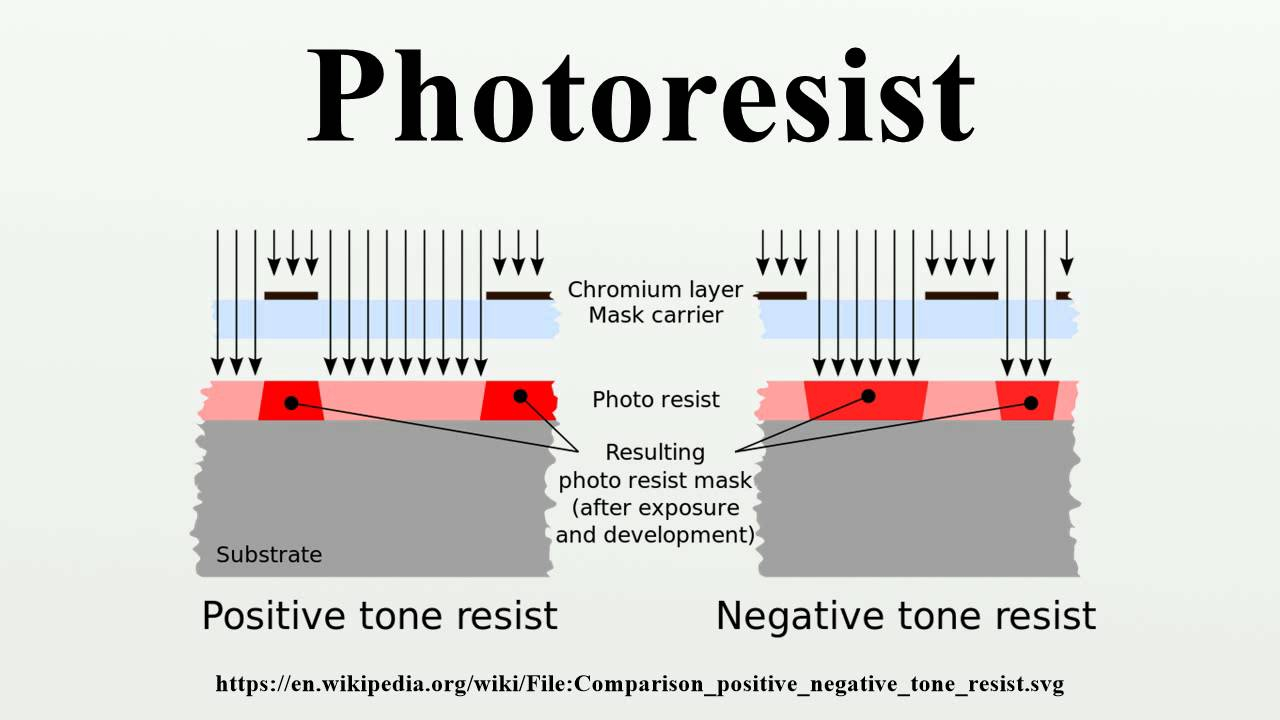
What is the difference between KrF and ArF photoresists? KrF (Krypton Fluoride) resists are used for 248nm wavelength lithography, while ArF (Argon Fluoride) resists are used for 193nm, allowing for finer resolution and smaller chip features.
How does 5G technology influence the demand for these materials? 5G requires a high volume of radio-frequency (RF) filters and high-speed processors, both of which utilize advanced photoresists during their complex manufacturing processes.
➤➤➤Explore MRFR’s Related Ongoing Coverage In Semiconductor Industry:
Reconfigurable Intelligent Surfaces Ris Hardware Market
Advanced Metering Infrastructure Market
Ground Penetrating Radar Market
Non-Destructive Testing Services Market
4 Inches Semi Insulating Silicon Carbide Wafer Market
Electric Vehicle Battery Management System Market
Fingerprint Recognition Ceramic Cover Market