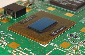
The global semiconductor packaging industry is undergoing an unprecedented architectural transformation as traditional wire bonding methods hit their physical limits regarding performance, signal integrity, and thermal dissipation. At the heart of this technological migration is an advanced microelectronics assembly method that reverses the semiconductor die to face downward, establishing direct electrical connections via microscopic conductive bumps. This structural shift completely eliminates the long wire loops characteristic of older packaging styles, resulting in a dramatic reduction in electrical inductance and a massive surge in signal transmission speeds. As consumer electronics become increasingly compact and demanding, from high-performance computing centers to next-generation smartphones, the pressure to pack more computing power into smaller form factors has never been higher. This has made advanced interconnect methods an absolute necessity for modern chip designers who are struggling to maintain the performance scaling promised by Moore’s Law. To properly navigate these tectonic shifts and comprehend the overarching trajectory of advanced packaging architectures, a rigorous and thorough Flip Chip Technology Market analysis is crucial for any technology stakeholder looking to build resilient, future-ready computing hardware.
Looking ahead, the widespread deployment of this advanced packaging technique is heavily catalyzed by the explosive growth of artificial intelligence applications and massive data center expansions worldwide. These complex, data-heavy workloads require ultra-fast processing speeds and high-density memory integrations that simply cannot operate on legacy packaging architectures due to severe thermal bottlenecks and latency delays. By facilitating direct, short electrical pathways between the chip and the substrate, this architecture offers superior thermal performance, allowing high-power processors to dissipate heat far more effectively into attached cooling structures. Furthermore, the integration of wafer-level packaging and copper pillar bumping technologies is pushing the boundaries of pitch density even further, allowing for thousands of microscopic connections on a single silicon die. However, manufacturing these sophisticated interconnects demands extreme precision and heavy capital investment in specialized cleanroom machinery, posing a significant entry barrier for smaller semiconductor foundries. As global supply chain players continue to consolidate, the organizations that successfully master high-yield bumping and advanced underfill material science will dictate the competitive landscape of the electronics sector for the next decade.
What is the primary mechanical advantage of face-down chip assembly over traditional wire bonding methods? Face-down assembly eliminates long, looped wire connections by utilizing microscopic conductive bumps placed directly across the entire surface of the die. This configuration dramatically shortens the electrical path, which drastically reduces parasitic inductance and resistance, thereby enabling significantly higher signal speeds, improved power delivery, and superior thermal dissipation properties.
Why are underfill materials considered critical to the long-term reliability of these packaging designs? Underfill materials are specialized epoxy resins injected between the silicon die and the substrate to encapsulate the delicate conductive bumps. This layer mitigates the intense mechanical stresses caused by the mismatched thermal expansion coefficients of silicon and organic substrates during temperature fluctuations, completely preventing solder joint fatigue and cracking.
➤➤➤Explore MRFR’s Related Ongoing Coverage In Semiconductor Industry:
Automatic Gate And Door Opening System Market
Automated Sortation System Market
Optical Fingerprint Sensor Market