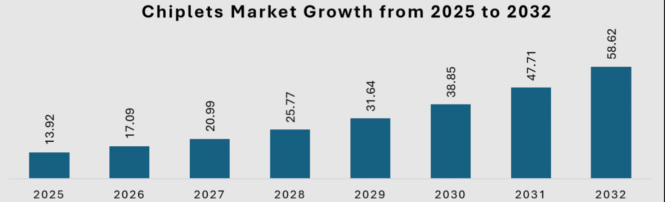
Global Chiplets Market Evaluated at USD 13.92 Billion in 2025, Projected to Surge past USD 58 Billion by 2032 as Semiconductor Design Shifts and AI Accelerators Explode
An elite global business intelligence, semiconductor vertical analysis, and commercial consulting corporation, has officially launched its highly comprehensive, data-backed industry study on the Global Chiplets Market . The exhaustive research publication offers an authoritative evaluation of the next-generation microelectronics design landscape, outlining critical structural growth drivers, packaging platform advancements, localized ecosystem initiatives, and strategic enterprise roadmaps across advanced computing industries.
The intensive market study demonstrates that the global chiplets sector stands at the absolute center of the most significant architectural evolution since the invention of the integrated circuit. Valued at USD 13.92 Billion in 2025, the market is tracking toward an estimated valuation of USD 58.62 Billion by 2032, expanding at an extraordinary Compound Annual Growth Rate (CAGR) of 22.8% during the forecast period. This remarkable hyper-growth trajectory represents a fundamental shift in the economics of Moore’s Law: as conventional monolithic die scaling becomes physically difficult and economically restrictive beyond the 3nm node, the semiconductor industry is adapting by using modular, heterogeneous integration to scale compute performance.
𝐃𝐨𝐰𝐧𝐥𝐨𝐚𝐝 𝐅𝐫𝐞𝐞 𝐏𝐃𝐅 𝐁𝐫𝐨𝐜𝐡𝐮𝐫𝐞 @https://www.maximizemarketresearch.com/request-sample/309075/
Executive Summary: Dismantling Monolithic Silicon for Modular High-Performance Computing
Modern high-performance applications have pushed standard, single-die semiconductor manufacturing to its physical limits. Designing a massive, single-piece silicon chip at advanced manufacturing nodes introduces severe economic liabilities. It results in reduced manufacturing yields, lengthy development cycles, and high mask costs. Furthermore, monolithic chips force non-compute elements—such as analog interfaces, I/O blocks, and physical memory controllers—to be produced on expensive, ultra-advanced nodes, even though these components do not scale effectively with finer process dimensions.
The modular chiplet architecture solves these design challenges by breaking a large system-on-chip (SoC) down into smaller, specialized functional tiles. Each individual tile—or chiplet—is manufactured on the specific process node best suited for its function, whether it is high-speed logic, power delivery, or memory management. These distinct pieces of silicon are then assembled onto a high-density substrate using advanced packaging technologies, acting as a single, unified high-performance processor.
The granular intelligence report analyzes the global chiplets market structure across several key categories to provide maximum clarity for industry stakeholders:
-
By Die Type: Logic Dies, High-Bandwidth Memory (HBM) Stacks, Analog & Mixed-Signal Dies, Photonic Interconnect Chiplets, and I/O Controller Modules.
-
By Integration Technology: 2.5D Interposer Packaging, 3D Vertical Die-on-Die Stacking, and Advanced Fan-Out Wafer-Level Packaging (FOWLP) systems.
-
By Packaging Platform: Silicon Interposers, Silicon Bridges (e.g., Intel's EMIB), High-Density Organic Substrates, and Glass-Based Interposers.
-
By End-Use Industry Vertical: Hyperscale Data Centers & AI Accelerators, Automotive Electronics (ADAs & Autonomous Driving Systems), Telecommunications Infrastructure, High-Performance Computing (HPC), and Premium Consumer Electronics.
Core Market Dynamics: Primary Economic and Technical Growth Drivers
An analytical review of the advanced electronic design space highlights several structural economic forces that are accelerating enterprise capital expenditure (CapEx) for chiplet deployment.
1. The Insatiable Compute Demand of Large AI Workloads
The rapid deployment of massive generative AI models and complex training clusters is the primary driver of the chiplets market. Monolithic die sizes are limited by the physical reticle limit of lithography equipment (typically around $858\text{ mm}^2$). Because advanced AI architectures require an immense number of transistors to process complex models, designers must link multiple compute dies together. Top-tier AI platforms use multi-die configurations to combine advanced logic chiplets with adjacent High-Bandwidth Memory (HBM) stacks, bypassing the physical constraints of single-chip manufacturing.
2. Radical Yield Optimization and Cost Minimization Mechanics
In semiconductor manufacturing, large monolithic chips are highly vulnerable to material defects; a single micro-imperfection can ruin an entire massive die, lowering factory yield and increasing unit costs. By disaggregating a massive chip layout into smaller functional chiplets, manufacturers can significantly improve silicon yields. Smaller dies naturally enjoy a higher probability of defect-free fabrication. Furthermore, non-critical communication interfaces and I/O blocks can remain on mature, reliable nodes (such as 7nm or 14nm), saving highly expensive advanced nodes (like 3nm or 2nm) exclusively for vital compute logic cores.
3. Open Standards and the Rise of the UCIe Ecosystem
Historically, multi-die architectures relied on expensive, proprietary interconnect fabrics, which limited their use to single-vendor ecosystems. The introduction of open standards, specifically the Universal Chiplet Interconnect Express (UCIe) specification, has changed the industry landscape. UCIe establishes standardized die-to-die physical layers and protocol stacks. This clear technological standard enables cross-foundry interoperability, allowing an enterprise to integrate a logic chiplet from one foundry with an analog or memory chiplet from another, creating a diverse market for commercial off-the-shelf chiplet components.
Technical Segment Analysis: Identifying High-Value Infrastructure Channels
High-Bandwidth Memory (HBM) and Logic Dies Lead Revenue Generation
By die type, Logic Dies and HBM Stacks command the largest share of overall market revenue. Logic chiplets serve as the central processing engine for modern multi-die systems, containing the highly dense transistor layouts needed for parallel processing. Concurrently, the HBM segment is experiencing substantial demand because modern generative AI models require vast memory bandwidth to avoid processing bottlenecks. Stacking DRAM memory layers vertically and connecting them directly to compute dies via high-density interconnects allows developers to achieve the memory throughput required for intense data center applications.
2.5D and 3D Packaging Technologies Dominate Integration Platforms
By integration technology, 2.5D and 3D packaging systems represent the dominant technical platforms. 2.5D configurations place functional tiles side-by-side on a high-density interposer or use localized silicon bridges (such as Intel's Embedded Multi-Die Interconnect Bridge) to handle critical routing. For applications requiring a compact physical footprint and low signal latency, 3D vertical die stacking is seeing increased deployment. 3D integration stacks memory or logic directly on top of base logic layers using Through-Silicon Vias (TSVs), minimizing wire lengths and significantly increasing die-to-die connection density.
𝐃𝐨𝐰𝐧𝐥𝐨𝐚𝐝 𝐅𝐫𝐞𝐞 𝐏𝐃𝐅 𝐁𝐫𝐨𝐜𝐡𝐮𝐫𝐞 @https://www.maximizemarketresearch.com/request-sample/309075/
Regional Developments: Geopolitical Investments and Advanced Packaging Hubs
North America: Leading Custom Silicon and High-Performance Design
North America holds the largest revenue position in the global chiplets market. This leading market presence is anchored by an established concentration of semiconductor design firms, major hyper-scale cloud providers, and active custom silicon programs in the United States. Prominent advanced graphics architectures, high-performance server processors, and cloud-native AI accelerators are designed primarily within this region. The regional focus centers on developing cutting-edge multi-die layouts, with major companies driving technology innovation to satisfy the compute demands of North American data center networks.
Asia-Pacific: The World's High-Velocity Foundry and Advanced Packaging Engine
The Asia-Pacific (APAC) region represents the fastest-growing market for chiplets, led by advanced semiconductor manufacturing hubs in Taiwan, South Korea, Japan, and mainland China. Taiwan’s premier foundries dictate global advanced packaging capacity through proprietary integration platforms like CoWoS (Chip-on-Wafer-on-Substrate). Concurrently, South Korea leads the global supply of advanced HBM memory. The region is seeing substantial capital investment driven by government-backed semiconductor manufacturing initiatives, making APAC the primary global hub for high-volume chiplet assembly, advanced substrate manufacturing, and final system testing.
Competitive Intelligence: Strategic Moves by Market Leaders
The global chiplets market features an intensive, high-stakes competitive environment where leading semiconductor foundries, fabless design firms, and advanced packaging providers invest heavily in technological innovation.
Key industry participants analyzed within the comprehensive market report include:-
1.Taiwan Semiconductor Manufacturing Company (TSMC),
2.Intel Corporation,
3.Advanced Micro Devices (AMD)
4.Samsung Electronics Co., Ltd.
5.NVIDIA Corporation
6.ASE Technology Holding Co., Ltd.
7.Amkor Technology, Inc.
8.Broadcom Inc.
9.Marvell Technology,
10.Qualcomm Incorporated.
The primary competitive strategies used by these industry leaders center on scaling advanced packaging capacity and expanding multi-die ecosystems:
-
Foundry Capacity Allocation: TSMC is aggressively scaling its advanced packaging facilities in Taiwan to meet the high demand for its CoWoS platforms, ensuring sufficient capacity for top-tier AI accelerator developers.
-
Architectural Shifts: AMD continues to leverage its multi-generation chiplet experience, utilizing advanced die disaggregation across its enterprise server and data center accelerator lines to maintain competitive performance advantages.
-
Integrated Device Manufacturing: Intel is establishing its automated packaging technologies, including EMIB and Foveros 3D integration, as core components of its foundry services, offering commercial clients flexible options for multi-vendor chiplet assembly.
-
Memory Integration Innovation: Samsung is utilizing its unique position as both an advanced memory manufacturer and a logic foundry to offer unified, turnkey chiplet solutions that bundle high-speed processing logic with next-generation HBM blocks on a single substrate.
For full access to the comprehensive strategic report, visit:https://www.maximizemarketresearch.com/market-report/chiplets-market/309075/
Industry Bottlenecks: Managing Thermal Dissipation and Test Complexity
Despite strong technological advantages, the widespread commercial adoption of chiplet architectures requires overcoming specific manufacturing and engineering challenges.
The primary technical challenge in high-density chiplet systems is thermal management and dissipation. Stacking multiple high-power logic dies vertically or placing them close together on an interposer creates concentrated hot spots. If these hot spots are not managed properly, uneven thermal expansion can warp the substrate and crack delicate die-to-die connections.
Additionally, testing multi-chip assemblies is highly complex. To prevent a single faulty component from ruining an entire multi-die processor, manufacturers must implement rigorous "Known Good Die" (KGD) testing protocols to verify each individual chiplet before final packaging, demanding advanced diagnostic tools and sophisticated quality control frameworks.
Strategic Outlook: The Transition to Photonic Interconnects and Glass Substrates
Looking forward, the global chiplets market is positioned to move beyond traditional copper-based interconnect structures. The next phase of microelectronics innovation will be defined by the commercial integration of Photonic Chiplets. By combining silicon photonic communication tiles directly with electronic compute dies, future processors can transition from copper wiring to optical light channels for chip-to-chip communication, unlocking massive bandwidth improvements while significantly reducing interconnect power consumption.
Furthermore, major packaging developers are transitioning from conventional organic substrates to Glass Substrates. Glass offers superior dimensional stability, flatter physical profiles, and excellent thermal resistance, allowing for closer routing tolerances and enabling the creation of larger, highly reliable multi-die systems. For corporate executives, technology directors, and product planners, adapting to this modular design shift is essential for maintaining long-term hardware competitiveness. Investing in flexible, standard-compliant chiplet ecosystems today ensures that enterprise computing infrastructure remains scalable, cost-effective, and powerful tomorrow.
About Maximize Market Research
Maximize Market Research is a multifaceted market research and consulting company with professionals from several industries. Some of the industries we cover include medical devices, pharmaceutical manufacturers, science and engineering, electronic components, industrial equipment, technology and communication, cars and automobiles, chemical products and substances, general merchandise, beverages, personal care, and automated systems. To mention a few, we provide market-verified industry estimations, technical trend analysis, crucial market research, strategic advice, competition analysis, production and demand analysis, and client impact studies.
Contact Maximize Market Research
3rd Floor, Navale IT Park, Phase 2
Pune Bangalore Highway, Narhe,
Pune, Maharashtra 411041, India
sales@maximizemarketresearch.com
+91 96071 95908, +91 9607365656